Understanding how different materials handle electric charge is fundamental in fields ranging from electronics to materials science. This knowledge hinges on the behavior of electrons within the materials; which varies significantly between conductors and insulators, as well as various states of matter. This article explores how conductors and insulators deal with electric charge. As well as introduces the concept of semiconductors and superconductors. Need a refresher on electric charge before getting into conductors and insulators? Check out the “What is Electric Charge” article.
Charge Mobility
A material’s ability to conduct electricity largely depends on the organization of its constituent particles and the freedom of charge carriers, such as electrons, to move through it. In liquids, particles are more loosely arranged. This allows ions and electrons to move relatively freely, which can facilitate conductivity under certain conditions. For instance, water is not a great conductor; however, adding electrolytes to the water can make the water much more conductive.

In gasses, particles are even less dense, making it extremely difficult for a current to flow in any meaningful direction. However, certain materials can be introduced to a gas to facilitate its transition into a plasma, allowing current flow. For instance, in neon tubes and high-pressure sodium bulbs, the introduction of materials like mercury allows current flow through a gaseous arc-tube.
We use mercury, because it has a relatively low ionization energy. Meaning it can easily release electrons when subjected to an electrical field. These free electrons then collide with the gas particles, ionizing them by knocking additional electrons free. This creates a plasma, a state of matter in which a significant portion of the gas is ionized, allowing current to flow through the gas. The resulting plasma emits light, which is why neon tubes and high-pressure sodium bulbs glow brightly.
In contrast, solids have more rigid structures where atoms or molecules are tightly packed, influencing the ease with which electrons can move. This lattice-type structure of solids is responsible for electric current flow in electrical conductors and circuits, and as so, the remainder of this article will focus on conductivity in solids.
Conductors and Insulators
Conductors are materials that allow the easy flow of electric charge, primarily facilitated by the movement of electrons. Typical conductors include most metals like copper, silver, and aluminum. Insulators, in contrast, are materials that resist the flow of electric charge, with electrons tightly bound to their atoms and unable to move freely. Common examples of insulators include rubber, glass, and most plastics.
Understanding why some materials are good conductors and others are good insulators requires examining the behavior of electrons within the material, governed by quantum mechanics and the structure of electron orbitals. In conductors, some electrons bind loosely to their atoms and move freely throughout the material. These are often referred to as “free electrons” or “delocalized electrons.” The presence of free electrons is a primary reason why materials like metals are good conductors of electricity. In insulators, electrons bind tightly within their respective orbitals and require a significant amount of energy to free them from their atomic structures. This binding prevents the free flow of charge through the material.
Metallic Bonding
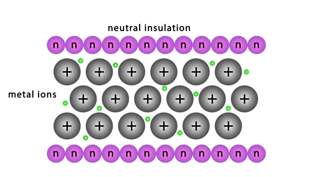
A unique arrangement known as a metallic lattice characterizes metals. This structure consists of metal atoms systematically organized in a repeating pattern. Each metal atom has electrons in its outermost shell, known as valence electrons. To achieve stability, metal atoms tend to lose these valence electrons, striving for a stable electron configuration similar to that of noble gases.

Unlike ionic or covalent bonding, where electrons transfer or share between specific atoms, metals exhibit a different phenomenon. In a metallic lattice, the valence electrons do not confine themselves to any particular atom. Instead, these electrons “delocalize,” forming what we refer to as a ‘sea of electrons’. This sea of delocalized electrons moves freely throughout the entire metal structure.
As metal atoms lose their valence electrons, they transform into positively charged ions, or cations. These cations remain fixed in place within the lattice, while the delocalized electrons drift freely around them. The electrostatic attraction between the positively charged metal ions and the negatively charged delocalized electrons constitutes metallic bonding. This type of bonding is fundamental to the properties of metals.
Insulating Barrier
The metallic lattice of copper facilitates the free movement of delocalized electrons. However, the interaction between these free electrons and the atoms in the insulating layer surrounding the copper conductor is fundamentally different. In insulating materials, electrons tightly bind to their respective atoms, as neutral atomic bonds primarily make up the insulating material. This strong binding arises from the significant energy required to remove an electron from its atomic orbit. Unlike in metals, where valence electrons can move freely, in insulators, these electrons confine to specific atoms, forming stable bonds that contribute to the material’s insulating properties.
Preventing Current-Flow
For a free electron in the copper conductor to cross into the insulating material, it would need to overcome a substantial energy barrier. This barrier exists because of the strong electrostatic forces holding the electrons within the atoms of the insulator. The energy required to dislodge an electron from the insulating material’s atoms is much higher than the thermal energy available under most practical conditions. Consequently, this prevents the free electrons in the conductor from moving into the insulation. But this also highlights the importance of taking care of conductor insulation while pulling wire. Any damage to insulation may allow these free electrons to flow out of the insulation, creating “leakage” which may allow them to travel on another conductive surface on the other side of the insulation barrier.

Additionally, in a conductor, delocalized electrons can move freely because there are available energy states they can occupy. In contrast, in insulators, the energy states that electrons could potentially move to are typically at much higher energy levels. Far above the conduction band. This significant energy gap means that, under normal conditions, there are no accessible energy states for the electrons to transition into within the insulating material.
The insulating layer serves as a physical barrier that separates the conductive material from external environments, including other conductive paths. The structure of insulators often results in an electrostatic repulsion effect. Which further inhibits any movement of free electrons into the insulation. This barrier ensures that the electrical current remains confined within the conductor, maintaining the efficiency and safety of electrical systems.
Copper Conductors
We commonly use copper conductors in electrical circuits because of its excellent conductivity and relatively low cost. Copper atoms have 29 electrons, but only the one electron in their outermost shell can move freely when an electric field is applied. In a copper wire, when a voltage is applied across its ends, the atoms making up the overall wire remain stationary. The field influences the free electrons, allowing them to gain energy and start moving towards the positive end, creating an electric current through the copper wire.

Thermoset Insulators
Insulators are materials that do not allow the free flow of electric charge. Their atomic structure tightly binds electrons, preventing them from moving freely. This makes insulators ideal for preventing the flow of electric current to pass through the material. A common example of an insulating material used in electrical applications is thermoset plastic. Such as cross-linked polyethylene (XLPE), used to surround electrical conductors. This is the protective black, red, white, or green insulation around some conductors electricians install.

In an insulator like XLPE, the electrons tightly bind to their respective atoms and do not move freely. When an electric field applies, the electrons do not move significantly, preventing current from flowing through the material. In the case of XLPE surrounding a copper conductor, the XLPE prevents the current from escaping the copper wire. Ensuring that electricity flows only through the conductor and not into the surrounding environment. This property is crucial for the safety and reliability of electrical systems, as it prevents short circuits and electrical shocks.
Semiconductors and Superconductors
Beyond standard conductors and insulators, there are other materials with unique properties that enable specific and advanced functionalities in electrical and electronic systems. These materials, known as semiconductors and superconductors, play crucial roles in modern technology. Semiconductors are the backbone of electronic devices, enabling the control and amplification of electrical signals. While superconductors offer unparalleled efficiency in power transmission and magnetic applications. Due to their ability to conduct electricity without resistance under certain conditions.
Semiconductors
Semiconductors are materials with electrical properties that fall between conductors and insulators. They can conduct electricity under certain conditions, such as the presence of impurities or exposure to light or heat. Semiconductors are the foundation of modern electronics, including diodes, transistors, and integrated circuits.
Silicon is the most widely used semiconductor material. In pure silicon, each atom forms covalent bonds with its neighbors. Creating a crystal lattice with no free electrons at low temperatures. When impurities (dopants) are added, they introduce free charge carriers:
- N-type Semiconductors: Doping silicon with elements like phosphorus adds extra electrons, slightly increasing conductivity.
- P-type Semiconductors: Doping with elements like boron creates “holes” (missing electrons) that act as positive charge carriers.
When an electric field applies, electrons in N-type semiconductors and holes in P-type semiconductors move, allowing current to flow. This controlled conductivity makes semiconductors versatile for various electronic applications where maintaining small, precise quantities of current is necessary.


Superconductors
Superconductors are materials that can conduct electricity with zero resistance below a certain temperature, known as the critical temperature. This property allows superconductors to carry large currents without energy loss.
Materials like niobium-titanium (NbTi) are commonly used superconductors. In a superconductor, below the critical temperature, electrons pair up to form Cooper pairs. These pairs move through the lattice structure without scattering, as would happen in a standard copper conductor, resulting in zero electrical resistance. An electric current can flow indefinitely without any energy loss when introduced. However, the downside to superconductors is that they require incredibly low temperatures to operate. For example, in niobium-titanium (NbTi), this critical temperature is around 10 Kelvin (-263.15°C or -441.67°F). To establish this temperature, mechanical processes must be in place to cool the conductors which, in turn, demands a significant amount of energy to maintain such an environment. Applications requiring highly efficient power transmission, such as MRI machines and particle accelerators, use superconductors.
Conclusion
The distinction between conductors and insulators lies in the behavior of their electrons, specifically in how these electrons distribute across energy bands. Band theory provides a comprehensive framework for understanding this behavior, explaining why some materials conduct electric charge more freely than others. As science advances, the manipulation of these properties becomes increasingly sophisticated, leading to innovations in electronics, energy efficiency, and materials science, fundamentally shaping the technological landscape of the future.